Products
- Multilayer PCB[10]
- Other PCB & PCBA[10]
Contact Us
- Contact Person : Ms. Han Mandy
- Company Name : Shenzhen Hengchengxin Circuit Board Co., Ltd.
- Tel : 86-0755-28095569
- Fax : 86-0755-29040581
- Address : Guangdong,Shenzhen,(Office) 325 Complex Building, Junction Of Industrial West Road And Zhonghuan Road, Minzhi Street, Bao'an Dist.
- Country/Region : China
- Zip : 518000
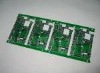
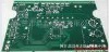
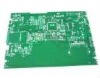
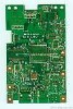
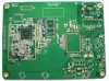
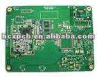
BEST high frequency PCB


Product Detailed
Related Categories:Multilayer PCB
Related Product Searches:BEST high frequency PCB,High Quality,rogers high frequency pcb, 10 layer motherboard pcb,HCX-0010
1. 1-12 layer fpc service
2. Small order or large order welcome
3. Prompt delivery
4.Good Quality
5.High precision
Related Product Searches:BEST high frequency PCB,High Quality,rogers high frequency pcb, 10 layer motherboard pcb,HCX-0010
General Manufacturing Capability:
| Gerber files- preferred | 274-X,274-D,DPF,ODB++ |
| Drill file | X & Y coordinates, with tool sizes included |
| Max. finished dimensions | 580mm x 800mm – Single/ Double-sided |
| 550mm x 800mm – Multilayer | |
| Standard | 1.6mm ±10% |
| Min. | Single/ Double-sided:0.2mm ±0.1mm 4-layer:0.4mm ±0.1mm 6-layer:0.6mm ±0.1mm 8-Layer:1.0mm ±0.1mm 10-layer:1.0mm ±0.12mm 12-layer:1.2mm ±0.12mm …32-layer:4.0mm ±0.4mm and above |
| Max. | 6.3mm ±10% |
| Bow and twist | < 7/1000 |
| Outer Cu weight | 1oz ~ 10oz |
| Inner Cu wight | 1/3oz ~ 6oz |
| FR4(High TG,halogen-free),FR5,ISOLA(FR408,370HR),TEFLON,POLYIMIDE,ROGERS(RO4003,RO4350,RO4450),Aluminum plate (Single,Double-sided) | |
| FR4 Thickness | 1.6mm |
| High TG FR4 (170 deg C) | 1.6mm |
| Max. number of layers | 32 |
| Min. thickness for inner layers (Cu thickness are excluded) | 0.07mm |
| Min. size | 0.1mm |
| Max. size | 6.0mm |
| Drill Deviation | ±0.002” (0.050mm) |
| PTH hole tolerance | ±0.003” (0.075mm) |
| NPTH hole tolerance | ±0.002” (0.050mm) |
| Angle of Countersink | 80°,90°,100°,120° |
| Min. hole size | 0.0008” |
| Aspect ratio | 20 |
| Trace width tolerance | ±20% |
| Min. trace width / space (1oz finished Cu weight starting from 1/3oz) | 0.003”/ 0.003”(0.08mm) |
| Min. trace width / space (1oz finished Cu weight starting from 1/2oz) | 0.004”/ 0.004”(0.1mm) |
| Min. trace width / space (2oz finished Cu weight) | 0.005”/ 0.005”(0.127mm) |
| Min. trace width / space (3oz finished Cu weight) | 0.008”/ 0.008”(0.2mm) |
| Min. trace width / space (4oz finished Cu weight) | 0.012”/ 0.012” (0.3mm) |
| Min. space from drilling to inner pattern | 0.1mm |
| Min. space from annular ring to inner pattern | 0.1mm |
| Layer-to-layer registration | ±0.003”(0.08mm) |
| Color | green,light green,matte green,white,extreme white,black,matte black,dark brown,yellow,red,blue,transparent |
| Min. solder mask clearance | 0.003” |
| Thickness | 0.0004” |
| Color | White,black,yellow,red,blue,green |
| Min. trace width | 0.005” |
| Min. size | 0.028” / 0.028” |
| AOI | Y |
| Flying Probe Tester | Y |
| Tolerance | ±10% |
| Impedance tester | Tektronix TDS8200 |
| End Mills Test | ±0.15mm(0.006”) |
| CNC Tolerance | ±0.15mm(0.006”) |
| V-Cut Depth | ±0.1mm(0.004”) |
| V-cut angle deviation | ±0.1mm(0.004”) |
| Semi-hole | Y |
| HASL,HASL pb free,immersion gold,immersion silver,immersion tin,O.S.P (Entek),S/G plating,ENEPIG,G/F plating,carbon… | |
| 3+N+3 | Y |
| Resin,hole-filling ink,PTH | Y |
| UL Cert. | Y |
| ISO Cert. | ISO9001/ISO14001/RoHS |
BEST high frequency PCB
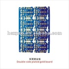
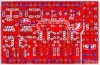
Other products